Reverse Bias Circuit Diagram
Zener diode forward and reverse bias circuit diagram Premium vector Circuit diagram: a) forward bias: (0-200 ma 1 κω w
What is Forward Bias and Reverse Bias? Example, Applications - ETechnoG
Reverse bias circuit diagram Reverse diode junction semiconductor capacitance pn biased biasing avalanche diodes physics depletion breakdown region voltage zener transition type bias forward (i) with the help of circuit diagrams distinguish between forward
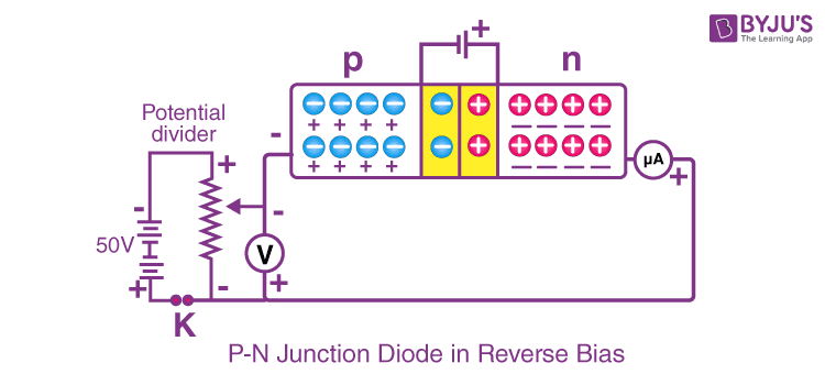
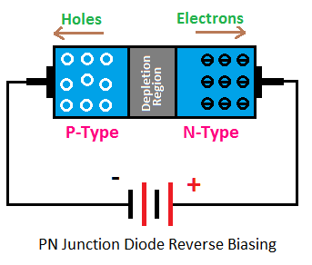
Pn junction under reverse bias condition
Diode forward bias circuit diagramElectronics: pn jnction diode under reverse bias Reverse bias circuit diagramBias junction biased diode.
Forward bias circuit diagramReverse bias circuit diagram Bias reverse diode forward junction circuit draw diagrams ii sarthaks voltage throughPn junction diode.

Reverse bias circuit diagram
Forward and reverse bias of a pn junction explained electrical4uForward biased circuit diagram Circuit diagram of zener diode in forward biasReverse bias pn junction circuit diagram.
Biasing difference bias diode voltagePn junction forward bias circuit diagram (a) draw the circuit diagrams of a p-n junction diode in (i) forwardElectronic – why is the voltage across the depletion layer higher than.

Get 42 zener diode reverse bias circuit diagram
What is reverse bias p n junction?Semiconductor physics Reverse bias circuit diagramJunction bias pn.
To draw the i-v characteristic curve of a p-n junction in forward biasStudy of forward and reverse characteristics of a pn junction diode. Forward biased circuit diagramDiode pn junction semiconductor reverse bias layer depletion characteristics working flow circuit notes current region physics electronics battery choose board.
Difference between forward & reverse biasing with comparison chart
Pn junction forward bias circuit diagramBias biasing diode etechnog pn depletion junction Reverse forward circuit diode biasing junction bias diagrams distinguish between sarthaks help characteristics iiWhat is forward bias and reverse bias? example, applications.
Forward and reverse bias circuit diagramForward and reverse bias circuit diagram Forward and reverse bias circuit diagramReverse bias circuit diagram practice.

Forward bias circuit diagram
.
.


